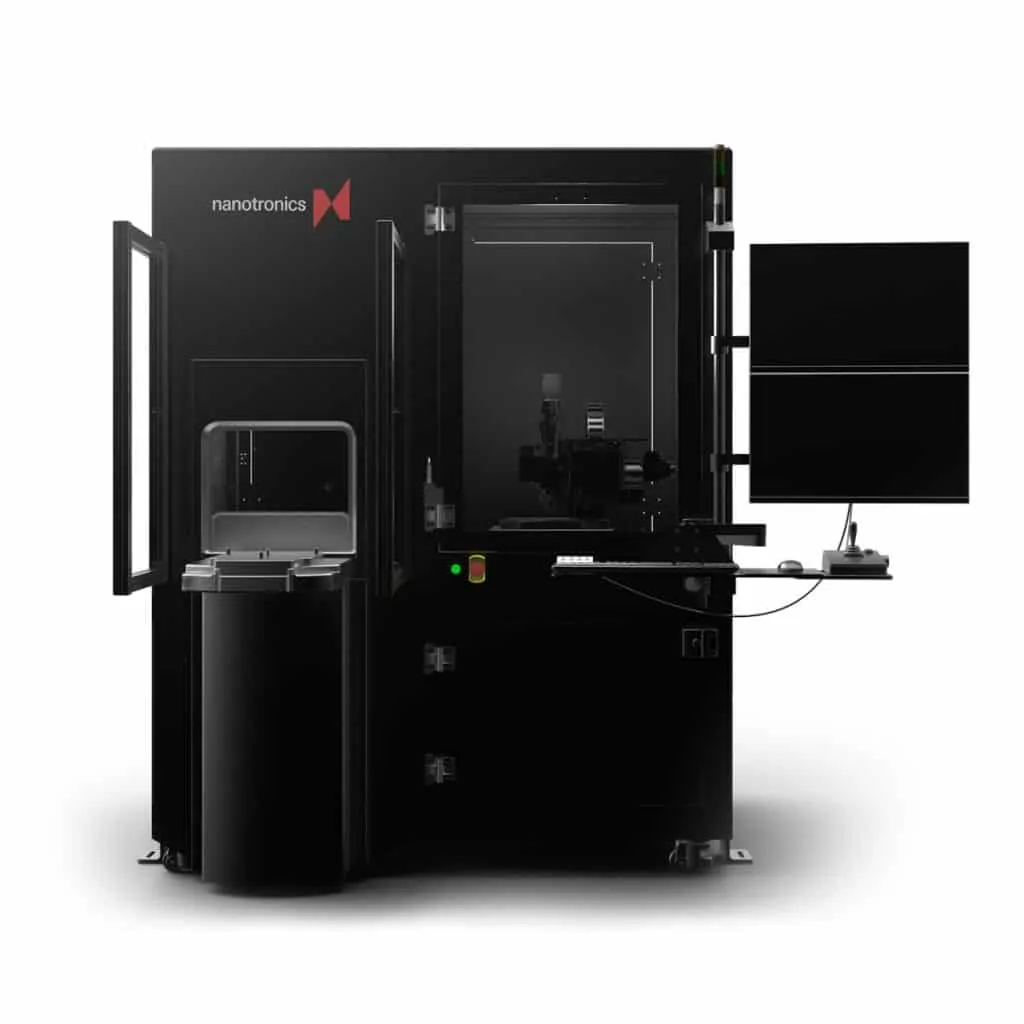
System
Weight
540 kg
Dimensions (W x D x H)
158 cm x 173 cm x 202 cm
Min. Vaccum Requirement
24 in. Hg (70 kPa)
Power Supply
110v/220v, 30 amps
Wafer Loader
Runs One Cassette at a Time:
25 wafers per cassette or FOUP
Standard Wafer Sizes
300, 200mm with adapter
Pre-Aligner
Optics
Illumination Modes:
Brightfield, Darkfield, DIC (Nomarski)
Light Source
White-light LED, Other options available
Objectives
2.5, 5, 10, 20, or 50x, user selectable
Stage
Travel, Typical
350 mm X and Y direction
Positioning
Linear servo motors with closed loop encoders (50 nm resolution)
Repeatability
+/- 0.5 μm
Travel Flatness
20 μm
Construction:
Precision ground raceways and high-rigidity linear guideways
Mounting Platform
Isolated platform integrated into cabinet system
Centered Load Capacity:
5 kg
Options
AFM
SECS/GEM
OCR Camera
Air Ionizers