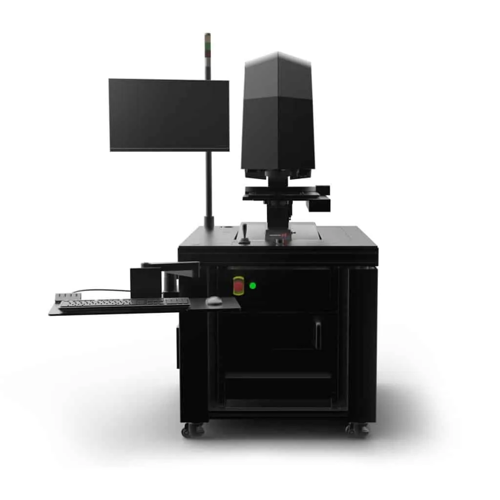
nSpec® LS
General
Features
Combining optical microscopy, computational super resolution, artificial intelligence, and robotics, Nanotronics is bringing the world’s most advanced microscope to every manufacturing sector.
Travel, typical 200 mm X and Y direction
Centered Load Capability 2.27 kg
Repeatability +/- 0.5 μm
Step Size 0.04 μm
Travel Flatness 30 μm
Weight 54 kg
Limit Switches Mechanical, non-adjustable
Wafer Vacuum Chuck (optional) Adjustable to 50, 75, 100, 150, 200, or 300 mm
White Illumination: LED (other options available)
Brightfield/Darkfield Objectives: 5, 10, 20, or 50x, user selectable
Differential Interference Contrast: (Normarski)
Stage, Focus, Nosepiece, Illumination, Camera
Manual user operated
Multiple Resolution Settings
Rapid Scanning
Wafer Mosaicing
Customizable Defect Reports
Configuration Options for Wafer Size, Defect type, and Scan Resolution
Sample Chuck Sizes to Meet Specific Needs